Cleaning & Coating

It is our C&C Division that leads the semiconductor precision parts cleaning business.

Scroll Down
The first-tier player in precise
cleaning and coating of
semiconductor parts.
1st Tier Player
1st Tier Player

The C&C Division is the leader in the semiconductor precision parts cleaning and coating industry due to its customer-centric quality management. We deliver semiconductor equipment parts that have been ultra-precisely cleaned and coated using state-of-the-art technology, based on solid trust in our customers' products and reliable systems. With ultra-precise cleaning utilizing various techniques based on the kind and shape of the process reaction products and coatings that generate highly functional films of rare earth oxide materials, we increase the life of products and realize the conditions of the semiconductor manufacturing process.

Features

  • Customer-centered Solution
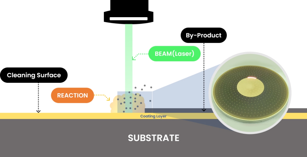
    • Providing tailored cleaning and coating technology through the quality management system
    • Using MES and a measurement/analysis system to achieve client satisfaction
    • Operating Real Time Monitoring System
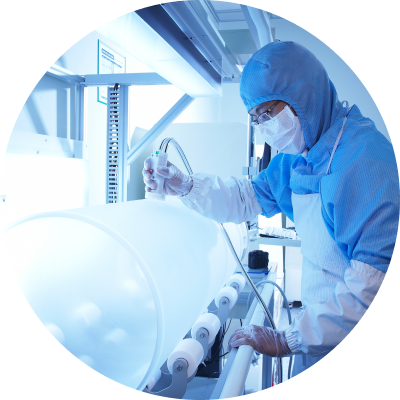
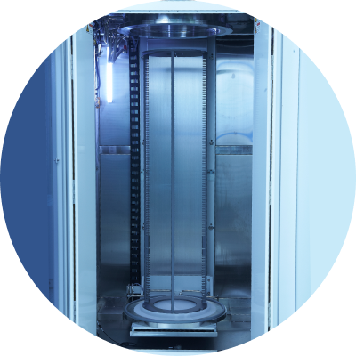
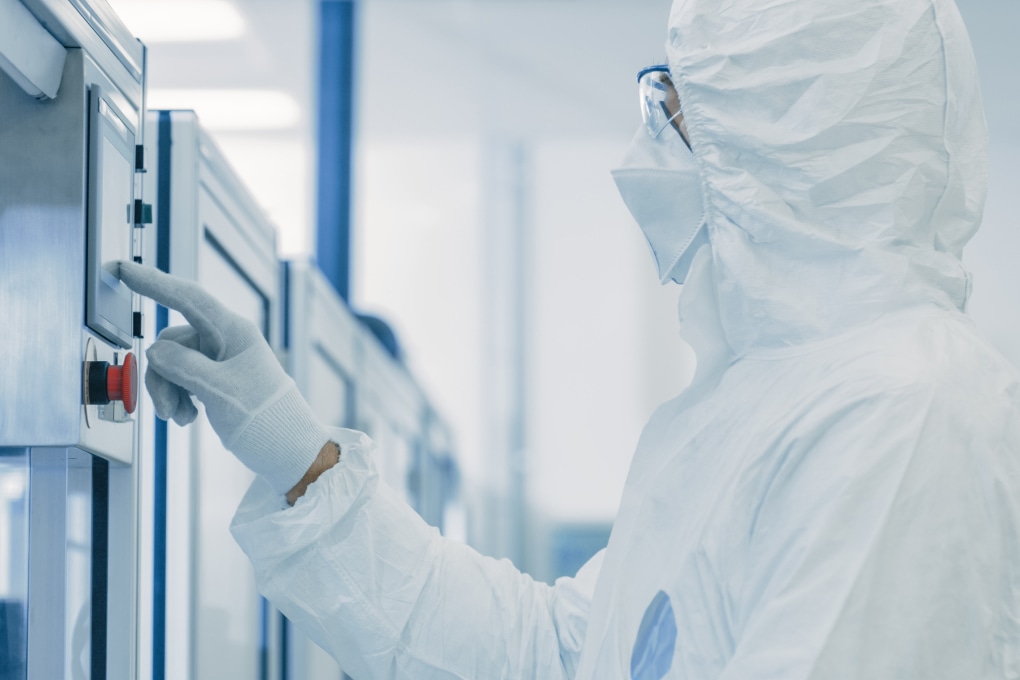
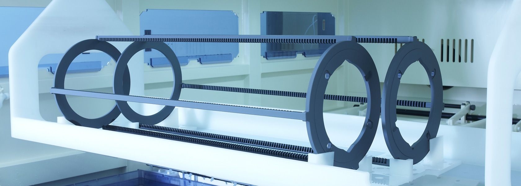
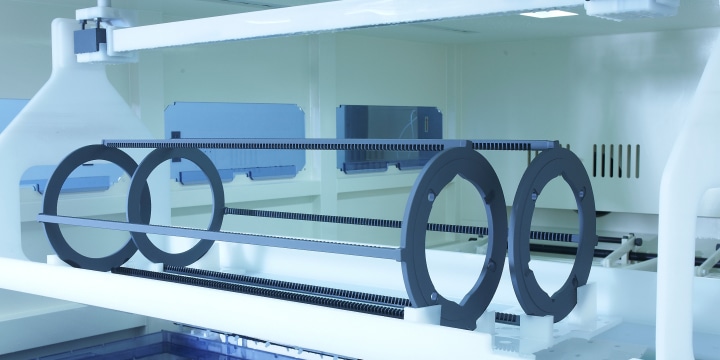
  • Maximizing our automated cleaning system
    • Constructing safe workplaces
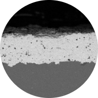
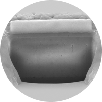
    • Delivering standardized product quality

C&C Location

  • Gumi Plant Gumi Plant
  • Anseong Plant Anseong Plant
  • Xi'an Plant Xi'an Plant

Process

  • Chemical Treatment
    Chemical Treatment
  • Inspection
    Inspection
  • Dry
    Dry

ECO

It is a cleaning procedure that uses a laser light energy source and irradiate laser beam
onto the surface of an object to remove contaminants on the surface.
eco

Coating Physical Property Table

Please check by moving to the left and the right. Please check by moving to the left and the right.
APS
APS
Division APS
Y2O3 Nano SB E-APS
Characteristic Outstanding plasma resistance Increased collection capacity of the reaction product ↑
Outstanding chemical resistance
Stabilized back-up time Outstanding chemical/physical resistance
Pore Density 3%↓ 3%↓ 2%↓ 1%↓
Hardness (Ratio) 1 (B.M) 2.2 0.8 1.9
Micro microstructure microstructure microstructure microstructure
Please check by moving to the left and the right. Please check by moving to the left and the right.
SPS&PVD
SPS&PVD
Division SPS PVD
Y₂O₃ I-SD I-SD H
Characteristic Outstanding durability of high-power plasma An upper part of chamber
Outstanding chemical/physical resistance
An upper part of a high-integration etching process
Outstanding chemical/physical resistance
Pore Density 0.5%↓ Near Zero
Hardness (Ratio) 2.0 2.7 3.6
Micro-structure microstructure microstructure microstructure